
[Free] Why Tiny Capacitors Became an AI Power Bottleneck
How AI GPUs turned a quiet component into a critical part of power delivery

Why MLCC Demand Exploded in the AI Era
The power story of the AI era usually begins with enormous numbers: gigawatt-scale data center demand, hundreds of kilowatts per rack, 800V DC, HVDC, substations, and new campuses built next to the grid. All of these matter. They describe a real shift in how power has to be brought to AI infrastructure. But they explain only one side of the bottleneck.
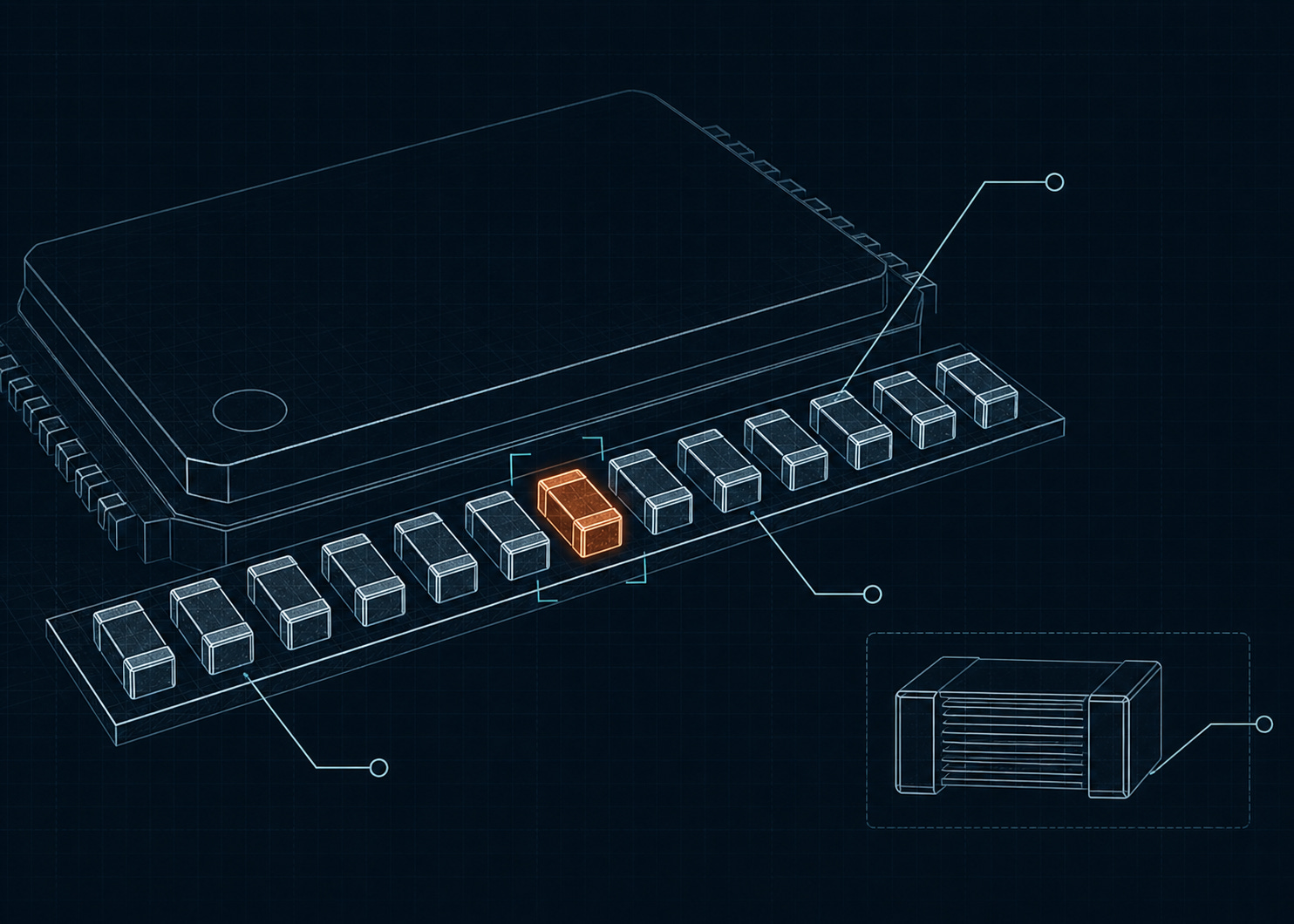
Something much smaller has been changing at the same time. A component that is almost invisible at the system level has quietly become part of the constraint: the chip capacitor. Around an AI GPU board, MLCCs can appear in the thousands. At the server level, that number can grow into the tens of thousands. Next to the story of substations and transmission lines, a component smaller than a fingernail has become part of the AI power problem.
Why did this happen? The common answer is simple: “Because the industry is moving to 800V.” That answer sounds intuitive, but it is not precise. To understand why MLCC demand exploded, we have to follow the power all the way down to the GPU, and then look at what happens just before it arrives.
Same Power, Different Bottlenecks
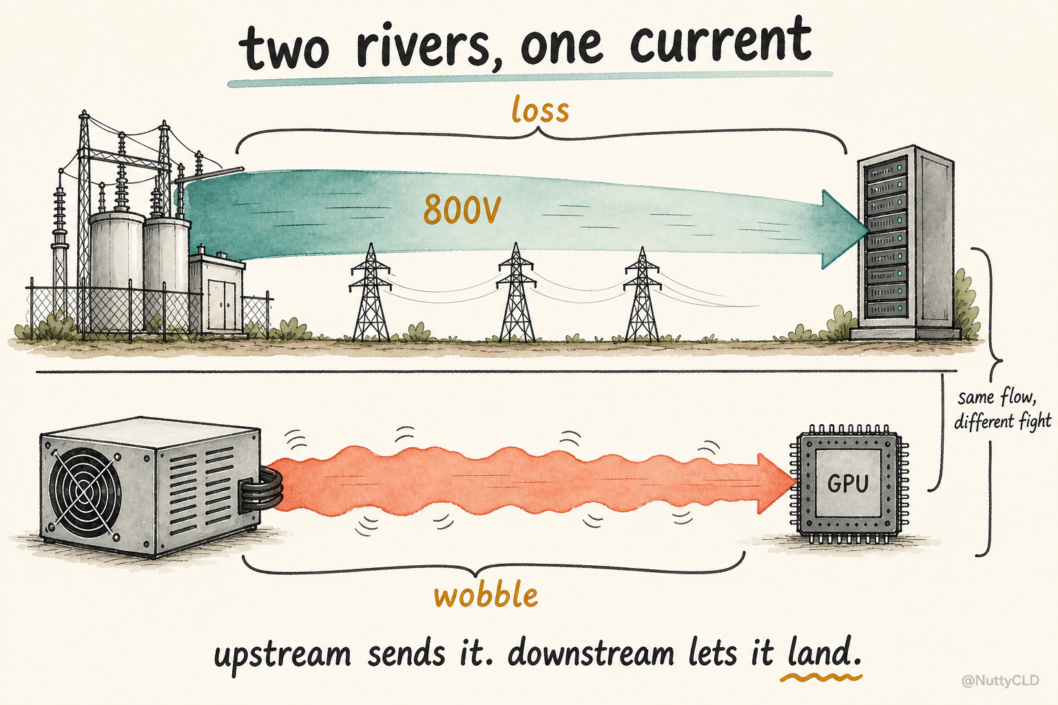
Power flows in one direction. But the problems it faces change completely depending on where you are in the system. Upstream power delivery is about moving a lot of power over distance, efficiently. Here, higher voltage helps. For the same amount of power, raising voltage lowers current, and lower current reduces cable loss and copper requirements. That is why AI racks are moving toward higher distribution voltages, with 800V DC sitting at the outer edge of that trend.
Downstream power delivery has to solve the opposite problem. Here, higher voltage is not the answer. The GPU core ultimately runs at sub-1V levels. Voltage is low, current is huge, and the load can change very quickly. So the same power system is fighting two different battles. Upstream fights loss. Downstream fights instability. MLCC demand exploded on the second battlefield.
The Last Centimeter
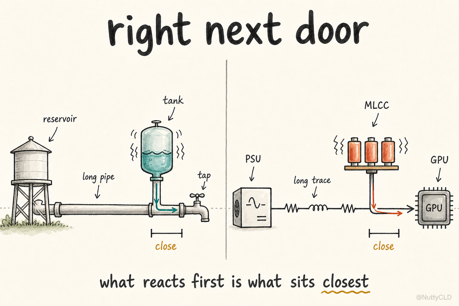
A water system gives the right intuition. Water starts at a large reservoir, travels through big pipes, enters a city, and finally reaches a faucet. But when someone suddenly opens the faucet, the distant reservoir cannot respond instantly. The pipes have length, inertia, and delay. Pressure changes take time to travel. If there is a small local tank near the faucet, the system behaves differently. When water is suddenly needed, the small tank responds first. When pressure fluctuates, it absorbs the shock locally.
MLCCs near a GPU solve a similar problem. When the GPU suddenly demands current, a distant power supply cannot respond instantly. The power path always has resistance, inductance, and delay. Switching inside the die creates fast current demand at nanosecond scales, while the board and VRM see load transients across a wider range of time domains. In either case, the distant source alone cannot keep up immediately. Local MLCCs respond first.
An MLCC is not a battery. It does not hold energy for seconds or minutes. It is a local buffer that releases or absorbs charge over very short time windows. It also helps shunt high-frequency ripple and suppress noise created by switching activity. Power arriving near the GPU is not enough. It must arrive on time, without excessive movement, and in a form the chip can actually use.
MLCCs are not long-duration energy storage devices. They are local timing devices for current.
From Waterfall to Delta
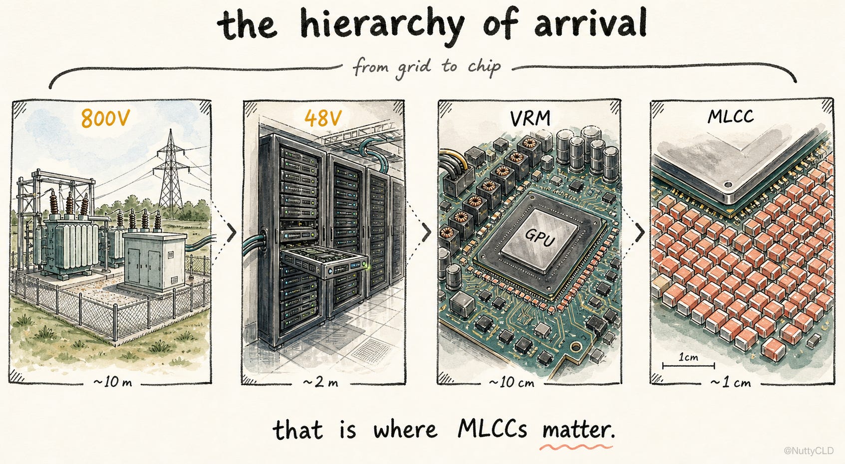
By the time power reaches the GPU, it has stepped down through several stages. In a traditional server power architecture, facility power passes through a PSU, then into an intermediate bus such as 12V or 48V, and finally through VRMs into the sub-1V rails used by the chip. Newer AI rack architectures add a higher distribution voltage, such as 800V DC, above that stack. Some architectures step down from 800V to 48V. Others discuss bypassing 48V and converting toward a lower intermediate rail such as 6V.
The intermediate stages can vary by architecture, but the destination is always the same: the sub-1V rail used by the GPU core. The process of converting one DC voltage into another is DC-DC conversion.
The basic relationship is simple:
P = V × I
At higher voltage, the same power can be delivered with lower current. When voltage falls, current must rise.
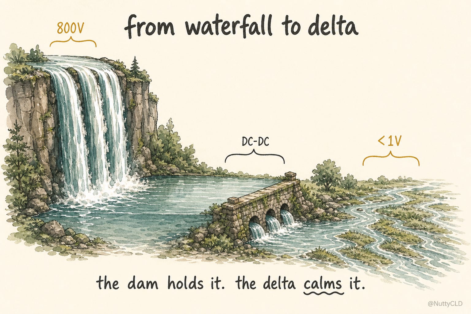
That is why 800V looks like a waterfall with a high drop. It lets the system move power efficiently with lower current. But the GPU core does not want a waterfall. It wants something closer to a river delta: low pressure, but enormous flow. The DC-DC converter transforms one into the other. It takes high-voltage, low-current power and rearranges it into low-voltage, high-current power. It is not simply throwing energy away. It is changing the combination of pressure and flow.
But the conversion is never perfectly smooth. A converter creates the desired average voltage and current by rapidly switching power on and off. It is like opening and closing a gate quickly to control average water flow. Every time the gate moves, the downstream flow and pressure fluctuate. In a power system, that appears as ripple and load-step transient behavior. MLCCs near the GPU act like small local buffer tanks near the final delta. When the flow shakes, they absorb the movement nearby and help turn the rough output of switching conversion into something the chip can actually use.
The Common Misunderstanding
At this point, one question naturally comes up. If the power system is moving toward 800V, did 800V cause the explosion in MLCC demand?
It is a tempting answer, but it is not the precise one. 800V is an upstream solution. As rack power rises, moving that power at lower voltage becomes increasingly difficult. Lower voltage means higher current. Higher current means higher I²R loss, thicker cables, more heat, and a less practical power distribution structure. So the voltage goes up.
800V is a way to move power efficiently toward the data center and rack. That upstream story — why 800V, why now — is its own essay.

It is like widening the highway. But 800V does not directly solve the high-current, fast-transient problem in front of the GPU. That problem remains in the domain of VRMs, PDNs, and MLCCs.
The causal chain is better understood this way: AI GPU scaling pressured both upstream and downstream power delivery at the same time. Upstream responded with higher-voltage distribution, including 800V DC. Downstream responded with stronger VRMs, tighter PDNs, and more aggressive decoupling.
So 800V and rising MLCC demand are not cause and effect in a direct sense. They are two outcomes of the same underlying force: AI GPUs demanding more power and faster transient response. That does not mean 800V is irrelevant. It enables higher rack power and larger GPU systems. Without upstream scaling, high-power GPU systems would have hit the wall earlier. If those systems could not scale, downstream MLCC demand would not have grown the same way.
800V did not create the demand for MLCCs. It enabled the system that would.
What the System Was Really Asking For
The question now becomes narrower. If larger GPU systems became possible, why did those systems need so many MLCCs? The common explanation is count-based: an AI GPU board uses a lot of MLCCs, and GPU shipments are rising, so demand goes up. That is not wrong, but it stops one layer too early.
Power delivery is not designed around component count. It is designed around a target impedance. Engineers first decide how much voltage movement the chip can tolerate when it suddenly demands more current. Then they design the power delivery network to satisfy that condition.
Most readers know V = IR. If current flows through resistance, voltage drops. Power delivery starts from the same idea, but here R is not just DC resistance. At high frequency, inductance and capacitance matter too. The problem becomes impedance, or Z.
The key PDN relationship is:
Z_target = ΔV / ΔI
The meaning is straightforward. If a load suddenly demands an additional ΔI of current, and the voltage is allowed to move by only ΔV, then the PDN impedance must stay below that target.
In AI GPUs, both sides move in the wrong direction at the same time. The current step gets larger, while the allowed voltage movement gets smaller. The numerator shrinks. The denominator grows. The target impedance falls sharply.
That is the real reason MLCC demand exploded. The system never asked for more capacitors as such. It asked for lower impedance. MLCCs happened to be one of the most practical ways to satisfy that demand near the chip.
The system did not ask for more capacitors. It demanded lower impedance.
Why It Became a Capacitor Problem
“Lower impedance” can sound abstract. Near the chip, in high-frequency power delivery, it becomes very concrete. When current is suddenly needed, the distant power source cannot respond immediately. Something has to fill the gap. For the short window in which voltage must not move too much, the closest available tool is capacitance.
Another simple equation helps:
i = C × dv/dt
This one line explains why MLCC count can rise so sharply. The GPU demands more instantaneous current. The allowable voltage movement becomes smaller. The system must respond over shorter time windows. To support a larger current step, with smaller voltage movement, over a shorter time, the system needs more effective capacitance close to the load.
This is not a contradiction. The goal is not capacitance itself. The goal is lower impedance. But in the last centimeter of an AI GPU power delivery network, MLCCs are one of the most important ways to realize that lower impedance physically.
Real PDN design is not just about adding capacitance. ESL and ESR shape self-resonance. Anti-resonance can damage broadband impedance. Package inductance changes the effective impedance seen by the die. Board layout and the VRM control loop determine the response of the full system.
But the direction is clear: larger current steps, smaller voltage tolerance, shorter response windows, lower impedance, and more MLCCs. In AI GPUs, these pressures moved together, in the same direction, at the same time.
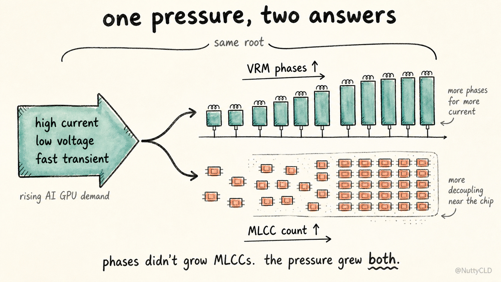
Same Pressure, Two Outcomes
VRMs faced the same pressure. As covered in The Last Few Centimeters, as AI GPU power rose, VRMs expanded into multiphase structures.

It is easy to look at that and say, “More phases, therefore more MLCCs.” The direction is roughly right, but the explanation is incomplete.
Multiphase VRMs can reduce ripple through interleaving. If we looked only at ripple, more phases might seem to reduce the need for output capacitance. But ripple is not the only reason phases increased. The real reason is current. A single phase cannot reasonably handle the current, thermal load, and transient response demanded by modern AI GPUs. Splitting the load across multiple phases distributes heat, shares current, and improves response.
As this happens, input decoupling near each power stage becomes more demanding. On the output side, the shared rail needs a denser decoupling network to meet the overall impedance target. More switching nodes appear. More local noise sources appear. Power conversion becomes more distributed and moves closer to the load. In the end, MLCC demand is not a simple function of phase count. It is a function of the impedance target.
Multiphase VRMs did not create the need for MLCCs. They scaled alongside it. The same pressure increased both phase count and MLCC count. That pressure has a name: high current, low voltage, fast transient.
AI Changed How Power Is Consumed
Explaining MLCC demand as “more AI servers” misses more than half the story. AI GPUs do consume more power. But the more important change is how they consume it.
Voltage fell. Current rose. Load transients became faster. Power conversion moved closer to the chip. The allowed voltage movement became smaller. Together, these changes pushed the PDN impedance target lower. In the last centimeter, the most practical way to meet that lower target was to place more effective capacitance closer to the load.
MLCC count went up because impedance had to go down.
At the system level, the hierarchy is clear. 800V is the highway for moving power over distance. 48V is a smaller distribution road. The VRM converts that power into a voltage the chip can actually use. And the MLCC is the small local buffer beside the final intersection, absorbing the movement before the flow reaches the load. What happens after the MLCC — the last micrometer into the die itself — is a different problem.

The AI power bottleneck is not only about bringing more electricity to the data center. It is also about making that electricity stable in the last centimeter. That last centimeter is defended by a component smaller than a fingernail.
That is where MLCCs matter.
Not because capacitors became exciting, but because AI made the last centimeter of power delivery impossible to ignore.
Disclaimer: This essay is for informational and educational purposes only. It is not investment advice and should not be interpreted as a recommendation to buy or sell any security. The technical explanations use analogies and simplifications to make the power-delivery architecture easier to follow. Real PDN design depends on many additional variables, including ESL, ESR, anti-resonance, package and board parasitics, layout constraints, thermal behavior, and control-loop dynamics.
Sharing Note: This article is free to read. Sharing the link is welcome. Short excerpts are also welcome with attribution and a link back to the original post. Please do not reproduce or republish the full article without permission.
samsung electro-mechanics?
I thought about Murata and Taiyo Yuden, but ultimately decided there were better plays out there.